

PCB Designing-Basics
Introduction
This is the first blog of the series to discuss and learn the basics of PCB designing. In this blog we will discuss, introduction and importance of PCB and its designing techniques. As well as we will discuss various software’s that are used for designing the PCB. Further we will design one small PCB for practice.
Importance and Introduction to PCB (Printed Circuit Board)
As an Engineer (of any field), whether is Mechanical Engineer, Computer Engineer or Civil Engineer, now and then everybody comes across the one of the vital part of respective industry i.e. Electronic Circuit. This electronic circuit is made or created on a special type of board, which is called PCB (Printed Circuit Board). Electronic circuits are very very critical as well as an important part of any given machinery.

As you can see in the above image, PCB is used to mechanically support and electrically connect electronic components using conductive pathways, which are usually called as Tracks. A PCB is a thin board made of Fiberglass, composite epoxy or other laminate material. Tracks are etched or printed onto a board, which connects different components on PCB, such as Transistors, Resistors, Capacitors and Integrated Circuits (IC).

These blue and red lines going criss-cross are the Tracks, which forms electrical connections between components. And these green and red objects are actually footprints or pads of components.
Now you’ve got a little bit of an idea about what exactly a PCB is… Right ?
So let’s move further and discuss, How to design the PCB.
Designing a PCB is an art and it requires lots of attention while designing it. Currently in the market you can see lots of EDA/CAD tools available. Most of them are licensed one, only a few of them are open source or freely available to use
PCB Designing Software :
1) Eagle
2) OrCAD
3) DIPTRACE
4) Proteus
5) KiCad
6) Altium Designer
7) Allegro
8) EasyEDA
These are some of the famous EDA software’s presently available in the market. One can use any one of the above lists as per their convenience of use. However every software has their own Pros and Cons.
So before discussing the PCB layouting, first we will discuss the process or different stages of PCB designing.
In order to design a PCB, one has to follow below steps :
- Create the schematic
- Link footprints to the components in schematic
- Generate a netlist
- Create desired PCB shape in PCB editor
- Import the netlist in PCB editor
- Define design rules
- Place the components footprint at desired location
- Route the tracks to form electrical connections between various components
- Add labels and identifiers on PCB
10.Generate design file
Schematic :A schematic diagram is a fundamentally two-dimensional circuit representation, showing the connectivity between different electrical components.
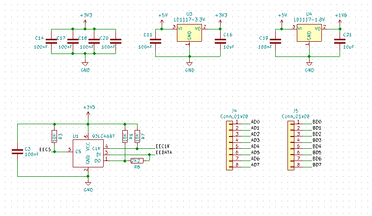
Above image shows various symbols, which actually represents the components used in that particular circuit. And every symbol has its unique name, like C14, U1, J4, R3 etc and the green lines make electrical connections between the components.
Symbols used in Schematic :
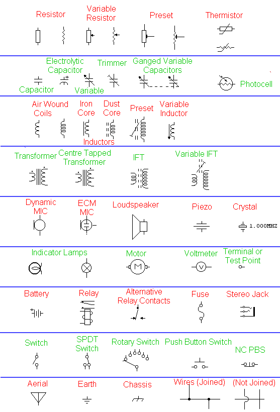
So these are some symbols which are used to prepare the schematic.
Netlist: The netlist contains the electrical connections between the components on the circuit board, and is usually held in textual format. In printed circuit board production a netlist (generated from the production data) is used to carry out an electrical test to find incorrect or missing connections.
Some EDA’s use these netlists to import components and connections from schematic to pcb design editor.
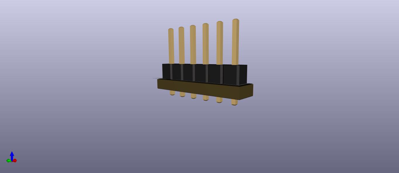
Footprint: In PCB design, a footprint is a pattern for an electronic component that will eventually be soldered there. Whether it is a through-hole component, a surface mount component or any connector, every part that gets soldered onto or into a printed circuit board needs a footprint.


PCB layers: A PCB is defined as a number of copper layers in a well-defined se quence. Copper layers of a PCB are usually just named LAYERS or also called SIGNAL layer. In general, a PCB is classified by the number of copper layers. Depending upon the size and complexity of circuits, a number of layers are defined. Boards that consists of 1 layer are often called: 1-layer or single sided PCB.

Above image is a representation of a single layer pcb. In which you can see copper tracks are at one side of pcb and on the other side only pcb footprints and legends are given.
So like this, if tracks are running from both sides of pcb then it is called 2 layer pcb.
Via: A via is used to make an electrical connection between the layers of a MultiLayer PCB. Connecting multiple layers of the board makes it possible to reduce the size of the PCB. A via is constructed by placing copper pads on each layer of the PCB and drilling a hole through them. The hole is made conductive through by placing copper cylinders directly in the drilled holes.
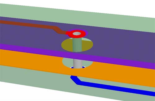
In above image you can see track from the top layer (Red) going through the pcb and ending on the bottom layer (Blue). so this is how Via works.
So these are some concepts used in pcb designing.
Now lets move to practically design the small PCB. We will use KiCad software to make this design. As KiCad is open source software it does not require any product license key for installation. it’s .exe files are easily available on the website https://kicad.org/download/.
After downloading .exe files, install the software on your PC or laptop

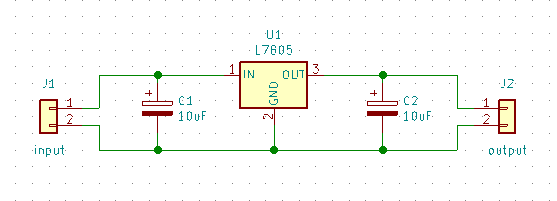
This is a small circuit which converts +12VDC input to +5VDC output using 7805 regulator IC.
To make the actual pcb of this circuit, first we have to create a project of it in KiCad.
- After installation of software open the software IDE.
- Go to File> New> Project > select or create destination folder > give name > press OK.
- Now you can see your new project IDE with two files .kicad_pcb and .sch files.
- First we have to make a schematic of the above circuit. So let’s open the .sch file.

This is how it will look like. We have to make circuits in this red rectangular area.This rectangular area is an actual representation of A4 page size.
- Above circuit consists of two connectors, two capacitors and one IC. To add these components in the IDE go to Place tab > symbols and then press on the page. Small window will popup where you have to choose your required components one by one.
- Select connectors, capacitors and IC one by one and arrange them on a sheet in proper sequence.
- To arrange the components on desired manner use following keyboard shortcuts
Move : press M,
Copy : press C,
Rotate : press R,
Drag : press G,
X mirror : press X,
Y mirror : press Y,
Place Wire : press W,
place Text : press T,
place label : L

- Now make an electrical connection between components and define their values and names. To make connections use the Wire tool.
- Next step is to attach the footprint to these symbols.
Go to Tools > Assign Footprint
Here you can see the list of your selected components. Now search the required footprints from the left side list and assign them to components.
Press OK and you will be redirected to the schematic window.

- So now we have to generate a netlist, in order to carry this schematic information to the PCB designing window.
Go to Tools > Generate Netlist File
Small window popups, just click on Generate Netlist. - Now go to the Main project window and click on .kicad_pcb file, where we will actually design our pcb.
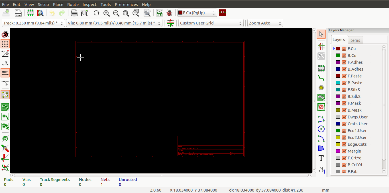
- On the right side table you can see various Layers. Each layer has its own functions. Here first we will define a board shape.
For that, first select the Edge cut layer and go to Place > Line. - Draw a rectangle or your desired shape of pcb. This shape is nothing but your actual pcb.
- select F. Cu layer again and go to Tools > Load Netlist > read current netlist.
- Now you can see the footprints of your components are loaded on your sheet.

- Now move and place the components inside this rectangle as per your convenience.
- Once you finish the components placement, then the next task is to Route the tracks on the PCB. To route the tracks go to Route > Single track.
- You can now connect the pins or pads of components with each other.
- If you select F. Cu layer then tracks w*ill be routed on Front Cu layer (RED tracks)
- If you select the B. Cu layer then tracks will be routed on the Bottom Cu layer (GREEN tracks).
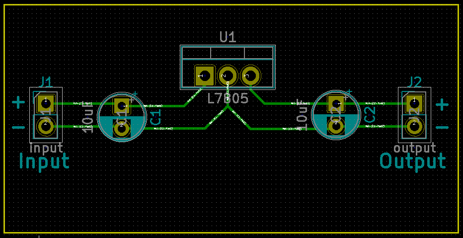
Here we have arranged the components as per our convenience and routed the Tracks from the Bottom side, hence these tracks are in green color.
- Go to Place > Text, to add the necessary Texts for understanding.
- Add Mounting holes for PCB :
Go to Place > Footprint > MountingHole_3.2mm. - And now you are ready to generate Design files which are commonly known as Gerber Files.
For making actual PCB, a PCB manufacturer requires these Gerber files. - To generate Gerber files go to File > Plot.
Here you have to select your destined folder to save your gerber files.
Do not make any changes in the remaining popup window and press PLOT. - Now we have to generate Drill Files. This you can also find in the same window.
Generate drill files in the same folder where you previously saved gerber files. - Congratulations…….!
You just have finished the PCB layout. - You can see the 3D view of the PCB.
Go to View > 3D Viewer.
Here you can see how exactly your PCB will look.
By pressing the left button of your mouse, you can change the direction of 3D view.

So this is how it will look like.
Summary
To summarize, in this blog first we did an introduction of PCB. Then we discussed various aspects related to it. We introduce the Basic Concepts of PCB like Schematic, PCB layers , etc. We discuss some of the PCB designing software currently used in the market. Then we moved further to make a small pcb for practice. And step by step we made a PCB.
References
- http://www.pic-control.com/pcb-design-service/
- https://qualityinspection.org/electronics-videos-basics-pcb-pcba-smt-process/
- https://kitflix.com/how-to-study-pcb-design-getting-started-with-printed-circuit-boards/
- http://www.csun.edu/~psk17793/S9CP/S9%20schematic_diagrams.htm
- http://www.jvdpcb.com/en/Product_detail.aspx?id=13
- http://www.pcb.electrosoft-engineering.com/04-articles-custom-system-design-and-pcb/01-printed-circuit-board-concepts/printed-circuit-board-pcb-concepts.html
- https://kicad.org/download/
- https://www.arduino.cc/
About Payatu
Payatu is a research-powered cybersecurity service and training organization specialized in IoT, embedded, mobile, cloud, infrastructure security, and advanced security training. We offer a full IoT/IIoTT ecosystem security assessment, including hardware, firmware, middleware, and application interfaces. If you are looking for security testing services then let’s talk, share your requirements: https://payatu.com/#getstarted Payatu is at the front line of IoT security research, with a great team, and in house tools like expliot.io. In the last 8+ years, Payatu has performed security assessments of 100+ IoT/IIoT product ecosystems and we understand the IoT ecosystem inside out. Get in touch with us. Click on the get started button below.

